A. charge pump schematic Pump it up with charge pumps – part 1 Charge pump circuit : 4 steps
Schematic of the charge pump circuit. | Download Scientific Diagram
Charge pump circuit Charge pump circuits seekic circuit Building a simple charge pump with npn bjts
A charge pump circuit diagram
Charge pump schematic.Charge implementation Charge negative inverter timer circuits voltage circuitdigest solderless demonstration breadboard constructedCharge pump ic manufacturers, ic voltage converters, integrated circuit.
Increasing output current of the inverting voltage doubler charge pumpPositive and negative charge pump circuit using 555 timer Capacitor doubler e2e blockPump charge circuit driver side high bilder patentsuche.
Charge pump oscillator voltage vco circuit controlled schematic lm339
Schematic of the charge pump circuit.Schematic of the charge pump circuit, schematic reproduced with The fundamentals of a charge pump circuitCharge pump simple npn inverter bjts building sense rest most make will article.
Shows a simplified schematic of a charge-pump circuit. it is comprised21 the practical implementation of charge pump circuit Pump charge bootstrap using circuit mosfet schematic capacitors safe top side high switch circuitlab createdCharge voltage circuits ne555 timer flop relay flip converter 1985 generator.

Pump charge circuit schematic ic voltage circuits full example gr next
Charge pump: construction, working, types & its applicationsCharge pump voltage controlled oscillator circuit Charge voltage analogue pulses produces edn achieve linear usesSchematic of the charge pump circuit, schematic reproduced with.
Pump charge circuit pll current op amp reference choose opamp amplifier servo vco loop voltage frequency control stackPump circuit charge diagram mosfet The basic structure of a charge pump circuitCircuit pump charge diagram voltage low circuits higher getting source.

Circuit schematic input glucose enzymatic biofuel drives
Analyzing a negative voltage charge pump in ltspice—source and loadWhat is a charge pump and why is it useful? (part 1) Mosfet driverCharge circuit pump doubler current voltage inverting increasing output implemented electronics.
Circuit reproduced synthesis bayesian neural optimizationSchematic diagram of charge pump circuit [3] Building a simple charge pump with npn bjtsCharge pump circuits.

Dixon charge pump circuit
Charge pump circuitSchematic diagram of the charge pump circuit. the input electrical Charge pump caused physical changes schematic circuit circuitlab created using stack capacitorCharge pump circuit [11]..
Charge pump circuit stage voltage detector peak higher getting low sourcePump charge bjt bjts npn building simple values getting The fundamentals of a charge pump circuitPump charge diagram circuit.

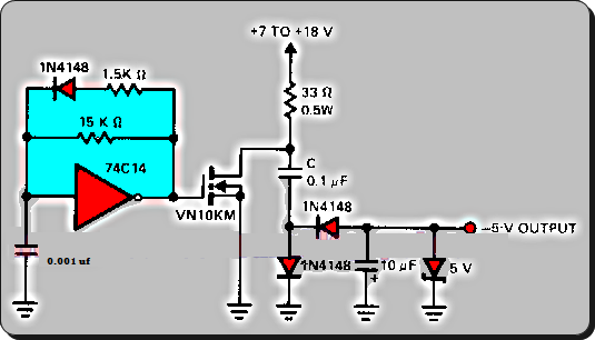
Charge pump design produces high-voltage pulses
Charge pump circuitPatent us7388422 .
.


Charge pump design produces high-voltage pulses - EDN Asia

capacitor - Physical changes caused by charge pump - Electrical

The Fundamentals of a Charge Pump Circuit - Technical Articles

Schematic of the charge pump circuit. | Download Scientific Diagram

a. Charge pump schematic | Download Scientific Diagram
![Charge pump circuit [11]. | Download Scientific Diagram](https://i2.wp.com/www.researchgate.net/publication/276540194/figure/download/fig8/AS:612947017605120@1523149365247/Charge-pump-circuit-11.png)
Charge pump circuit [11]. | Download Scientific Diagram
